- 您现在的位置:买卖IC网 > Sheet目录2010 > MAX5312EAE+T (Maxim Integrated Products)IC DAC 12BIT 5V/10V SER 16-SSOP
MAX5312
Data in the shift register is transferred to the input register
during the appropriate software command only. Data in
the input register is transferred to the DAC register in one
of two ways: using the software command, or through
external logic control using the asynchronous load input
(LDAC). Table 2 shows the software commands that
transfer the data from the shift register to the input and/or
DAC registers. The CLR, an external logic control, asyn-
chronously forces the input and DAC registers to zero
code, and the output to 0V, in both unipolar and bipolar
modes. The interface timing is shown in Figures 2 and 3.
Wait a minimum of 100ns after CS goes high before
implementing LDAC or CLR. If either of these logic
inputs activates during a data transfer, the incoming
data is corrupted and needs to be reloaded. For soft-
ware control only, connect LDAC and CLR high.
DAC Architecture
The MAX5312 uses an inverted DAC ladder architec-
ture to convert the digital input into an analog output
voltage. The digital input controls weighted-switches
that connect the DAC ladder nodes to either REF or
GND (Figure 4). The sum of the weights produces the
analog equivalent of the digital-input word and is then
buffered at the output.
±10V, 12-Bit, Serial, Voltage-Output DAC
14
______________________________________________________________________________________
CONTROL BITS
DATA BITS
MSB
LSB
C3
C2
C1
C0
D11
D10
D9
D8
D7
D6
D5
D4
D3
D2
D1
D0
Table 1. Serial-Data Format
CONTROL BITS*
INPUT DATA
C3
C2
C1
C0
D11–D0
FUNCTION
0
XXXXXXXXXXXX
No operation; command is ignored.
0
1
0
12-bit DAC data
Load input register from shift register; DAC output unchanged.
0
1
0
12-bit DAC data
Load input and DAC registers from shift register; DAC output updated.
0
1
0
XXXXXXXXXXXX
Load DAC register from input register; DAC output updated; input register unchanged.
1
0
XXXXXXXXXXXX
Enter shutdown; input and DAC registers unchanged.
1
0
XXXXXXXXXXXX
Exit shutdown; input and DAC registers unchanged.
Table 2. Serial-Interface Programming Commands
X = Don’t care.
*All unlisted commands are reserved commands. Do not use.
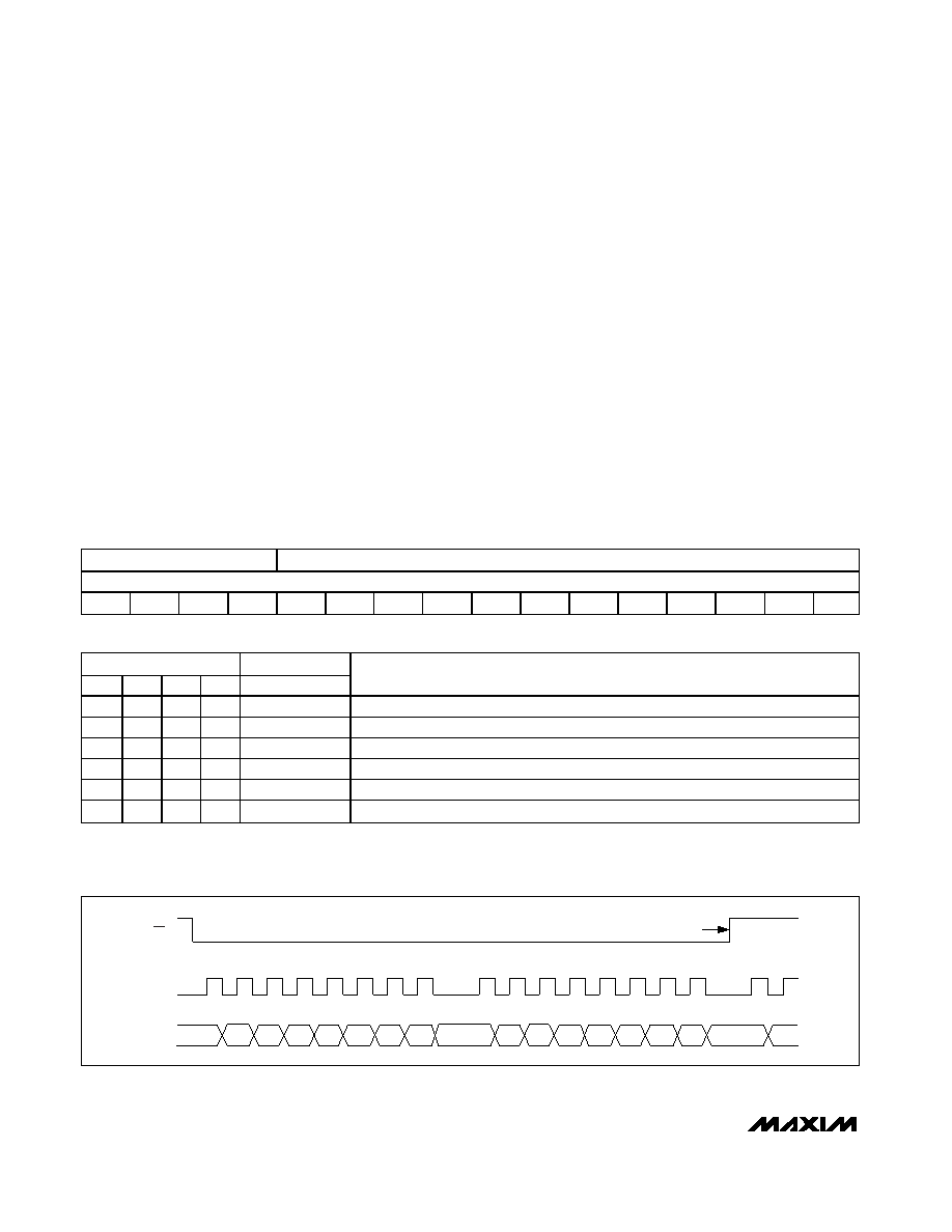
SCLK
DIN
COMMAND EXECUTED
9
8
16
(1)
1
C2
C3
D0
C1
C0
D11
D10
D9
D6
D5
D4
D3
D2
D1
D8
D7
CS
Figure 2. Serial-Interface Signals
发布紧急采购,3分钟左右您将得到回复。
相关PDF资料
MAX5316GTG+
IC DAC 16BIT SPI 24TQFN
MAX5322EAI+
IC DAC 12BIT DUAL 10V SER 28SSOP
MAX532AEPE+
IC MDAC 12BIT DUAL SER 16-DIP
MAX5355EUA+
IC DAC 10BIT 3.3V VOLT OUT 8UMAX
MAX5362PEUK+T
IC DAC 6BIT LP 2WIRE SER SOT23-5
MAX5365EUT+T
IC DAC 6BIT LP 3WIRE SER SOT23-6
MAX536BEWE+
IC DAC 12BIT QUAD CALIB 16-SOIC
MAX5380NEUK+T
IC DAC 8BIT 2WIRE SER SOT23-5
相关代理商/技术参数
MAX5312EAE-T
功能描述:数模转换器- DAC RoHS:否 制造商:Texas Instruments 转换器数量:1 DAC 输出端数量:1 转换速率:2 MSPs 分辨率:16 bit 接口类型:QSPI, SPI, Serial (3-Wire, Microwire) 稳定时间:1 us 最大工作温度:+ 85 C 安装风格:SMD/SMT 封装 / 箱体:SOIC-14 封装:Tube
MAX5312EVKIT+
功能描述:数据转换 IC 开发工具 MAX5312 Eval Kit
RoHS:否 制造商:Texas Instruments 产品:Demonstration Kits 类型:ADC 工具用于评估:ADS130E08 接口类型:SPI 工作电源电压:- 6 V to + 6 V
MAX5316GTG+
功能描述:数模转换器- DAC 16-bit V Out SPI DAC w/Digi Gain & Offset RoHS:否 制造商:Texas Instruments 转换器数量:1 DAC 输出端数量:1 转换速率:2 MSPs 分辨率:16 bit 接口类型:QSPI, SPI, Serial (3-Wire, Microwire) 稳定时间:1 us 最大工作温度:+ 85 C 安装风格:SMD/SMT 封装 / 箱体:SOIC-14 封装:Tube
MAX5316GTG+T
功能描述:数模转换器- DAC 16-bit V Out SPI DAC w/Digi Gain & Offset RoHS:否 制造商:Texas Instruments 转换器数量:1 DAC 输出端数量:1 转换速率:2 MSPs 分辨率:16 bit 接口类型:QSPI, SPI, Serial (3-Wire, Microwire) 稳定时间:1 us 最大工作温度:+ 85 C 安装风格:SMD/SMT 封装 / 箱体:SOIC-14 封装:Tube
MAX5317GTG+
功能描述:数模转换器- DAC 16Bit DAC w/Digital Gain/Offset Control RoHS:否 制造商:Texas Instruments 转换器数量:1 DAC 输出端数量:1 转换速率:2 MSPs 分辨率:16 bit 接口类型:QSPI, SPI, Serial (3-Wire, Microwire) 稳定时间:1 us 最大工作温度:+ 85 C 安装风格:SMD/SMT 封装 / 箱体:SOIC-14 封装:Tube
MAX5317GTG+T
功能描述:数模转换器- DAC 16Bit DAC w/Digital Gain/Offset Control RoHS:否 制造商:Texas Instruments 转换器数量:1 DAC 输出端数量:1 转换速率:2 MSPs 分辨率:16 bit 接口类型:QSPI, SPI, Serial (3-Wire, Microwire) 稳定时间:1 us 最大工作温度:+ 85 C 安装风格:SMD/SMT 封装 / 箱体:SOIC-14 封装:Tube
MAX5318GTG+
功能描述:数模转换器- DAC 18-bit V Out SPI DAC w/Digi Gain & Offset
RoHS:否 制造商:Texas Instruments 转换器数量:1 DAC 输出端数量:1 转换速率:2 MSPs 分辨率:16 bit 接口类型:QSPI, SPI, Serial (3-Wire, Microwire) 稳定时间:1 us 最大工作温度:+ 85 C 安装风格:SMD/SMT 封装 / 箱体:SOIC-14 封装:Tube
MAX5318GTG+T
功能描述:数模转换器- DAC 18-bit V Out SPI DAC w/Digi Gain & Offset
RoHS:否 制造商:Texas Instruments 转换器数量:1 DAC 输出端数量:1 转换速率:2 MSPs 分辨率:16 bit 接口类型:QSPI, SPI, Serial (3-Wire, Microwire) 稳定时间:1 us 最大工作温度:+ 85 C 安装风格:SMD/SMT 封装 / 箱体:SOIC-14 封装:Tube